Digital Systems
Implementation Technology
VLSI
"Very Large-Scale Integration" refers to circuit devices that contain thousands to millions of transistors.
Pros
- Complete control overall aspects of circuit implementation
- Can optimize for speed, area, power as needed
- Allows you to achieve highest device performance
- Cost effective for large volume designs
- Facilitates mixed-signal design
Cons
- Manufacturing is costly
- Mistakes are costly
- Verification process is long and thorough
- Design process is slow - long time to market
- Device functionality is static - no way to add system features
ASIC
"Application Specific Integrated Circuit" same manufacturing as VLSI, with reduced design time, made of predefined components. These libraries are accessed with a HDL based design and synthesis process, and then mapped to an implementation in the target technology.
Pros
- Faster design time than VLSI
- Some ability to optimize for speed, area, power as needed
- Allows you to achieve good device performance
- Can be cost effective for large volume designs
- Faster testing and verification than VLSI
Cons
- Manufacturing is costly
- Mistakes are costly
- Testing and verification is slow
- Design and manufacturing is slow - long time to market
- Once manufactured, device functionality is static - no way to add system features
Programmable Logic
Simple Programmable Logic Devices
Programmable logic forms were factory programmable such as ROMs and MPGAs (mask programmable gate arrays). The connection between these devices must be designed by the designer, which shortens design time compared to VLSI and ASIC.
ROMs/LUTs
ROMs were intended as memory devices (such as cartridges) but could be used for logic functions. ROMs can store a truth table to implement combinational logic. Each ROM has
PLAs/PLDs
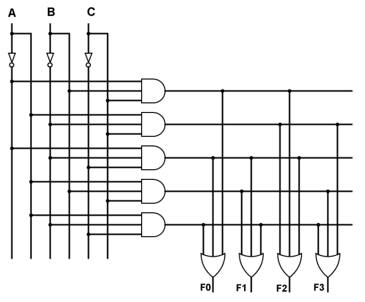
Programmable Logic Arrays (PLA) are based on the notion that any logic function is a combination of product terms OR'd together.
FPGAs
Field Programmable Gate Arrays are flexible programmable logic for larger designs. Complicated to program, but offer large capacities and flexibility.
- Programmable I/O blocks - Pin configuration
- Programmable Logic blocks - LUTs, AND-OR, multiplexers, etc.
- Programmable Routing Resources - Routing between the pins and blocks
Pros
- Faster design time than VLSI
- Reduced cost of design errors
- Flexibility for new requirements
- Cost effective when low number of devices
Cons
- Lower logic density (unused elements take up space)
- Higher power consumption
- Not applicable to all designs - floating point
Intro to VHDL
VHDL ("VHSIC" (Very High Speed Integrated Circuit) Hardwre Description Language) describes digital circuits but can be used to generate circuits automatically (synthesis). This facilitates top down design, and provides reusable elements and mature design practices. This can reduce the cost of prototyping complicated systems.
Timing
The after will ensure A and B are assigned to C 5 ns after being evaluated.
If a pulse occurs for less than 3 ns, it will be rejected. If longer than the rejection time, it will be propogated after a 5 ns delay. Inertial delay is the default delay assumed by VHDL.
Transport will delay the signals without rejecting.
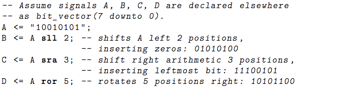
Data Types
- bit - 0, or 1
- bit vector - an array of 0, 1
- std logic - 0, 1, X, U, etc
- std logic vector - array of std logic
VHDL Modules
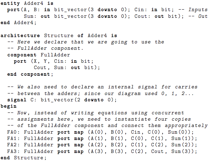
Entity similar to a function prototype. Describes port inpus and outputs.
Architecture is a description of the internals.
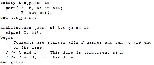
The devices can be reused in separate files by declaring it as a component and instantiating each element individually, assigning pins.
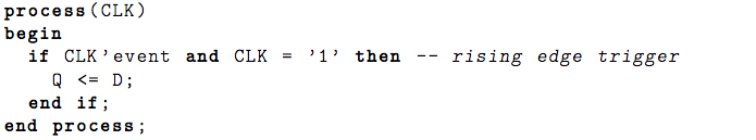
Sequential Statements
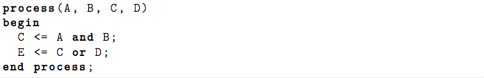
The process statement will monitor a signal using a sensitivity list and trigger a sequence of lines to be completed in order.
Flip Flops
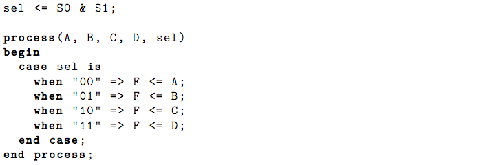
Conditional Assignments

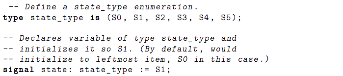
User Defined Types
Advanced Design
Logic Minimization
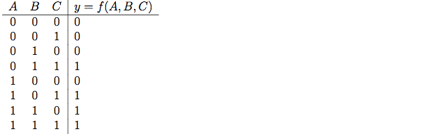
This is known as the Standard Sum of Products form - this can also incorporate Don't-Care:
Quine McCluskey Method
This reduces the SSOP form to a minimum sum of products by eliminating as many literals as possible to produce prime implicants, and then creating a chart of implicants to be OR'd to implement the original function.
Recall
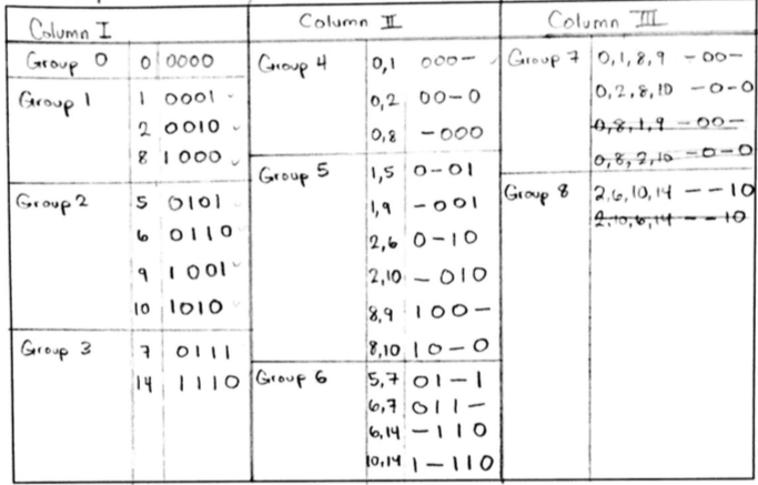
The numbers which don't reduce to the following column or are redundant are \textit{prime implicants}. In this case, the prime implicants are
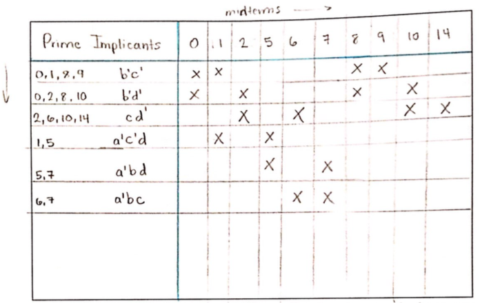
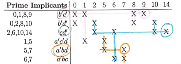
Choose the values with a single X in its column, then draw a horizontal line through the row. Any intersections, draw a vertical line. Continue until all X are crossed out, choosing values which will cover off as much as possible.
Hazards and Testing
Hazards in Combinational Circuits
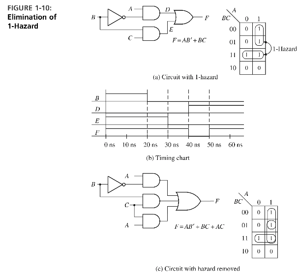
Static 1 Hazard
If a circuit goes 0 when it should have been 1
Static 0 Hazard
A circuit goes 1 when it should be constant 0
Dynamic Hazard
When the circuit should transition from 0 to 1 or 1 to 0, but transitions three or more times
Select inputs to test specific port errors:
Scan Testing
Memory and Arithmetic
More VHDL
System Design
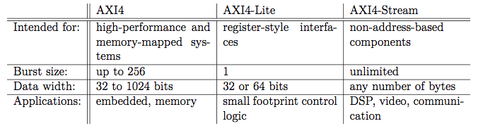
AMBA/AXI
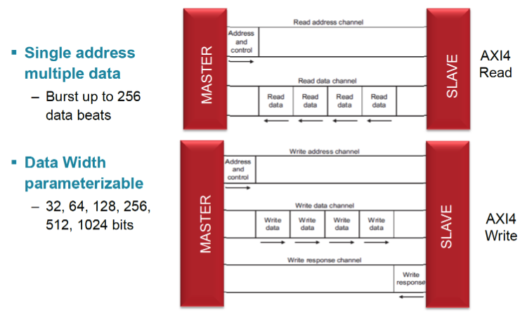
AMBA is a protocol created by ARM for components designed for other companies. This is an open standard on-chip interconnect for connection and management of blocks in a System-On-Chip.
AMBA has four interface protocols, AXI (Advanced Extemsible Interface), AHB (Advanced High Performance Bus), APB (Advanced Peripheral Bus), and ATB (Advanced Trace Bus).
AXI4-Lite is a subset of AXI4 used for simpler control register style interfaces. All transactions are burst legnths of 1, data accesses are the same size and width as the data bus, and exclusive access is not supported.
Channel is a collection of signals associated to a VALID signal.
Interface is a collection of 1 or more channels that expose an IP's core function. An IP core can have multiple interfaces.
Bus is a multiple bit signal (may be part of an interface or channel, but distinct).
Transfer is a single clock cycle where information is communicated qualified by a VALID handshake.
Transaction is a complete communication operator across a channel composed of one or more transfers.
Burst is a transaction consisting of more than 1 transfer.
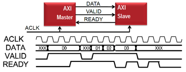
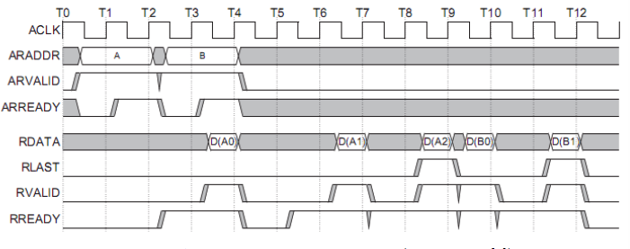
An AXI4 handshake is as follows:
- Master asserts a VALID when data is available
- Slave asserts READY if able to accept
- Date is transferred when VALID and READY
- If the transaction has more than 1 transfer, next data is sent, otherwise VALID is removed
- If slave cannot accept, READY is removed to pause
AXI4 and variants all have 5 basic signalling channels:
- Read address
- Read data
- Write address
- Write data
- Write response (Slave to Master)
For AXI-Lite, only 1 data tranfer per transaction.
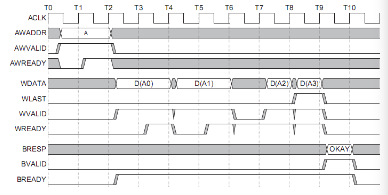
Write Address Channel (AXI4-Lite)
- AWVALID - The address write valid signal (master to slave)
- AWREADY - The address write ready signal (slave to master)
- AWADDR - The target write address
- AWPROT - The protection type specifying privilege and security level
Write Data Channel (AXI4-Lite)
- WVALID - The data write valid signal (master to slave)
- WREADY - The data write ready signal (slave to master)
- WDATA - The n-bit write data
- WSTRB - The write strobe lines indicate with bytes hold valid data (1 bti for each 8 bit data)
Write Response Channel (AXI4-Lite)
- BVALID - The write response valid signal (slave to master)
- BREADY - The write reponse ready signal (master to slave)
- BRESP - Write reponse indicating state of transaction
Read Address Channel (AXI4-Lite)
- ARVALID - The address read valid signal (master to slave)
- ARREADY - The address read ready signal (slave to master)
- ARADDR - The target read address
- ARPROT - The protection type specifying privilege and security level
Read Data Channel (AXI4-Lite)
- RVALID - The data read valid signal (master to slave)
- RREADY - The data read ready signal (slave to master)
- RDATA - The n-bit read data
- RRESP - Read response associated with the data, similar to BRESP
Off-Chip Protocols
Serial Peripheral Interface
Synchronous serial communication used for short distance communication in embedded systems. Uses a master-slave architecture with one or more slaves.
Four signals:
- SCLK - Clock signal that synchronizes data to clock edges
- MOSI - Master-out-Slave-in serial data line (master to slave)
- MISO - Master-in-Slave-Out serial data from slave to master
- SS - Slave select chooses which slave to communicate with
Communication protocol for attaching low-speed peripheral controllers. Short-distance intra-board communication. Multiple masters and slaves with bidirectional lines, Serial Data Line (SDA) and Serial Clock Line (SCL).
Four modes of operation:
- Master transmit
- Master receive
- Slave transmit
- Slave receive